| ▲ Electronics |
I figured it was about time that I described my own experiences with making PCBs. This is not intended to be an in-depth step-by-step guide - there is plenty of information already out there. I've just described briefly what works for me.
Credit where credit is due - when I first started, I followed the fantastic guide at Mike's Electric Stuff's page on "How to make really really good homemade PCBs". He has far more information there, and I'd strongly suggest you start by reading his page first.
My printer is an HP Laserjet 1160. When printing anything, use the manual feed tray and a straight-through paper path.
Lay out your PCB in whatever program you're happiest using (I use Eagle). Make sure that track widths, ground plane isolation, hole sizes etc all conform to the design rules you're using. The most useful I've found is Sparkfun's - see here. Do everything in inches - it will make your life easier in the end.
Here's a few sizes I use:
Holes - 0.6mm (24mil) for vias, 0.8mm (32mil) for most leaded components, 1mm (40mil) for PCB pins, pin headeres, TO-220 cases, big diodes etc.
Pad diameter - for vias (24mil hole), 50mil minimum (40mil is possible, but not advised). Most components with 32mil hole - 66mil. ICs and other components where tracks need to pass between pads - 56mil.
Tracks - generally as wide as possible. Minimum 16mil. Obviously, surface-mount boards may require thinner.
I used to think this was a really awkward technique, but I can now see its advantages. Mainly, the ability to use plain copper-clad board (no expired photoresist) and no need for a developing stage. It can also be used for applying silkscreen logos. A while ago, I discovered that it was possible to laser-print on to a piece of silicone paper and then iron it on to the board, giving perfect toner transfer and adhesion. Here are some options.
Silicone paper (or the backing paper from self-adhesive labels). This initially gave best results. However, when I switched to a cheapo toner cartridge in my printer, it simply did not stick to the silicone paper! There is obviously something better about branded toner - it stuck perfectly. Print the pattern on to a sheet of normal paper first. Then, cut out a piece of silicone paper and stick it with Scotch 3M Magic Tape over the printed area, and feed it back through. Silicone paper is too slippery to feed properly, so the carrier paper is used to feed it through. Iron/laminate on, cool, and peel off gently.
"Proper" transfer paper. Have a look at www.pcbfx.com. This looks great stuff and is available in the UK from Cool Components. The transfer paper is dextrin-based, so is completely water-soluble. There are alterative water-soluble papers available (for example, from http://www.barnyarns.co.uk/Soluble-Fabric-Paper-c-2177.html which is for embroidery, quilting etc.) but I don't know how well they'd work for toner transfer. Print, iron/laminate, and soak. This leaves the toner on the board. Then, iron/laminate a sheet of toner reactive foil on top. This basically adds yet more material to the toner, ensuring a solid coat. It can also be used to apply a coloured silkscreen!
Magazine paper. A cheap alternative, which works quite well, is to print the design on to a piece of really cheap/thin magazine paper. You'll probably need to tape it to a carrier paper (like with the silicone paper) since it's too flimsy to feed by itself. Clean the PCB and give the entire board a quick dip in etchant to "bite" the surface and roughen it slightly (it will turn dull). After ironing the paper on, leave to soak in warm water for 10min or so and gently rub off the paper. If you're careful, you can get a pretty good toner coating left behind. Because this is bare toner and came off a rough surface (the magazine paper), you will get pinholes, so I wouldn't recommend it for fine work. You could apply toner reactive foil on top, but if you're doing that, you might as well have used the proper dextrin paper anyway. If you were really careful and arranged some sort of alignment jig, it might be possible to iron on a second identical layer of toner to fill in any pinholes.
By far the best, if you have the equipment. Best for double-sided boards, since you can ensure alignment of the transparencies beforehand.
Choice of substrate. Get presensitised board - don't even think about trying to use spray photoresist, it's an absolute mess (if you really must apply photoresist to an uncoated substrate, think about using dry-film resist, widely available on EBay. It works great.). You can use FR4 laminate, which is solid fiberglass-epoxy composite, but I prefer using "economy" board which is a SRBP (resin-bonded paper) core with a fiberglass facing. This is much more forgiving on drill bits than solid fiberglass. I have seen photoresist-coated SRBP boards, but I find that the copper adhesion is much worse on SRPB than on fiberglass and you can lift tracks/pads easily.
Transparency preparation. Print using a laser printer on to tracing paper. If you can do 600dpi or better, that's great. Adjust your printer's settings to apply the maximum amount of toner, and turn off any toner-saving features. As per Mike's Electric Stuff, I use Gateway tracing paper, Viking Direct order code Q29-RG1059. For best results, use branded toner - cheapo toner can be less dense. If in doubt, you can print two identical transparencies and stack them - I do this quite often, since it ensures good coverage in solid areas like ground planes.
Expose board. Using a UV exposure box, expose the board. For double-sided boards, use some sort of jig to hold the transparencies, such as this one I made.
Develop. DO NOT USE SODIUM HYDROXIDE. PERIOD. I tried using this, and that's why all my boards were useless. It is too sensitive, and can easily strip all the resist off before you realise. Instead, use a silicate-based developer. For sources, see Mike's Electric Stuff page again. It works really fast (10-15s) at room temperature (I made up half the recommended strength, and it still works fast). To check if it's fully developed, rinse and dip briefly in the etchant. If it goes dull over all the exposed areas, you're ready to etch.
Etch. I swear by ferric chloride etchant. I've never tried anything else, and I'm not going to! However, if you have another etchant you like (e.g. persulphate, or peroxide/acid), by all means, go for it. Ferric chloride, warmed to 40°C, will etch a board in 5-10 min with gentle agitation in a tray.
Cleanup/prep/tinning. Once etched, remove the photoresist with conc. sodium hydroxide. Rinse, dry, and give the board a quick buff with a polishing block. Drill your holes. Tinning - totally optional. I never found it helped soldering much, but it can make boards look nicer. Tinning solutions don't last long, so it's a bit of a wasteful process.
Soldering. I use either leaded or lead-free, but mainly leaded since it flows so much better. Flux - I use "Fluxite" brand plumber's flux, loaded into a syringe. What, I hear you say? Yes, it's meant for plumbing, but I love it for PCBs. It does contain zinc chloride, so make sure to wash off all residues afterwards to prevent corrosion. To be honest, I've never tried any other paste flux. For flux removal, I use Ecosolve 300 from Surclean. It contains isohexene and rips through flux residues instantly. After that, hot water and detergent, then a blow-dry with compressed air leaves a squeaky-clean board. Bits of stripboard circuits I soldered over 12 years ago with Fluxite flux, while they now look a bit crap, show no signs of any corrosion, so I don't think Fluxite is bad.
I have since switched to using Warton Brown Flux Jelly (http://www.warton-metals.co.uk/brown-jelly.html). It is easier to remove than Fluxite (comes off with isopropanol) and, in some cases, seems to work a bit better. One downside is that it's a bit runny & sticky and tends to get everywhere.
When soldering both sides of a component on a double-sided board, there is a tendency for flux trapped around the wire in the hole to splutter and cause bubbling in the solder. To avoid this, I often solder the top side first, since it's more visible and should look nicer, and then solder the bottom side, but only very quickly so the flux doesn't have a chance to boil too much.
Vias. I use a 0.6mm hole for vias - nice neat fit for solid-core equipment wire. With care, you can get nothing more than a "bump" showing on both sides. Solder one side, snip the wire off, sand down with a little grinding stone on the Dremel, then solder the other side. Some photos below.Obviously, for components like resistors, you can solder on both sides of the board, so try and make use of them for leading signals through the board. See this page for a test of via sizes.
Here's a self-indulgent gallery of some boards I've made over the past few years. They're roughly in chronological order.
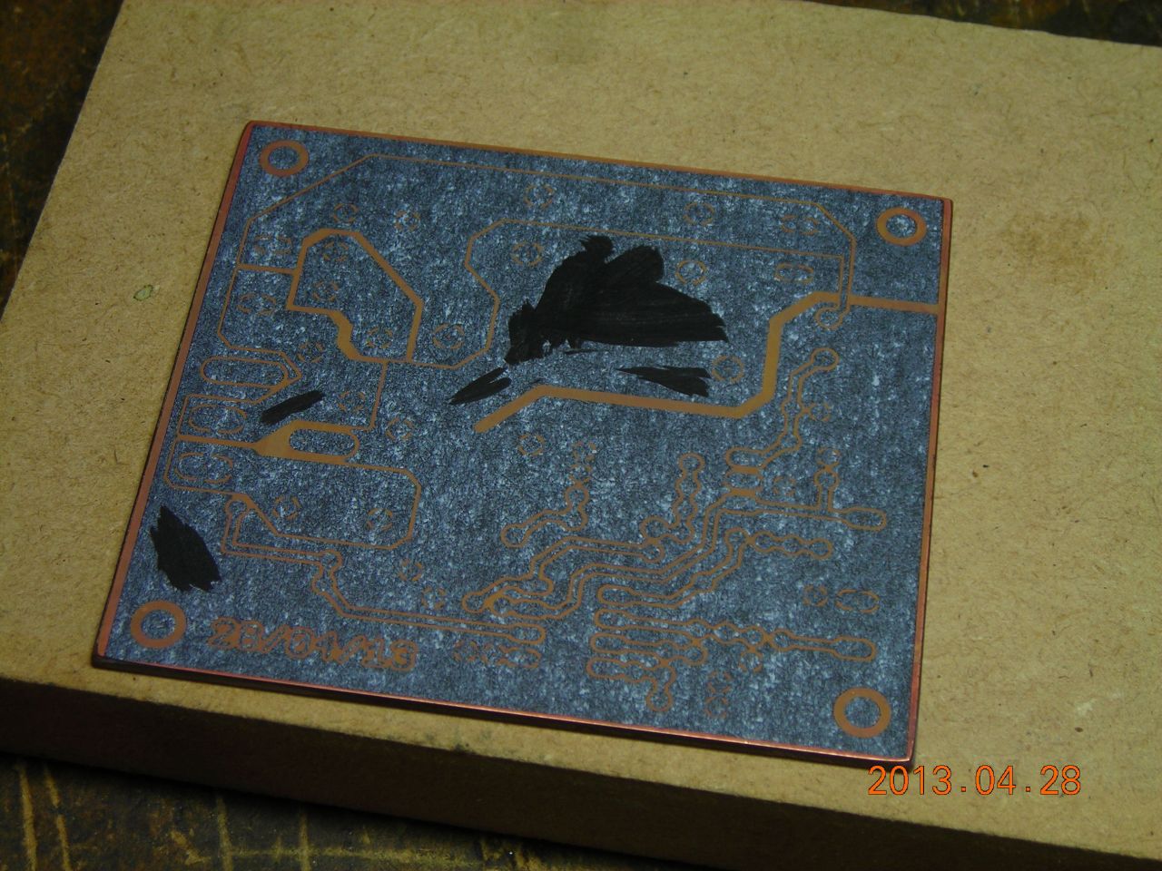
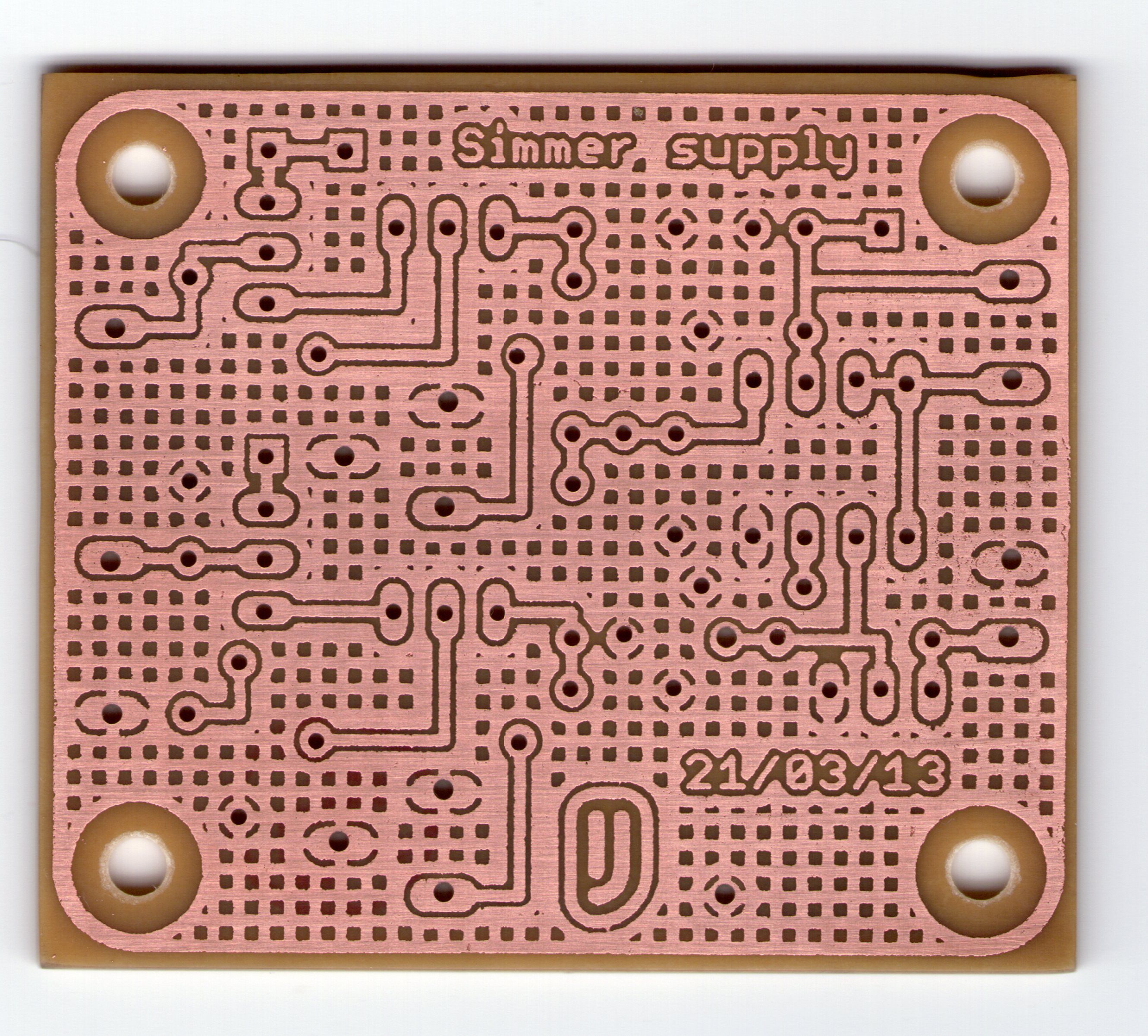 Toner transfer on SRPB board (magazine paper) |
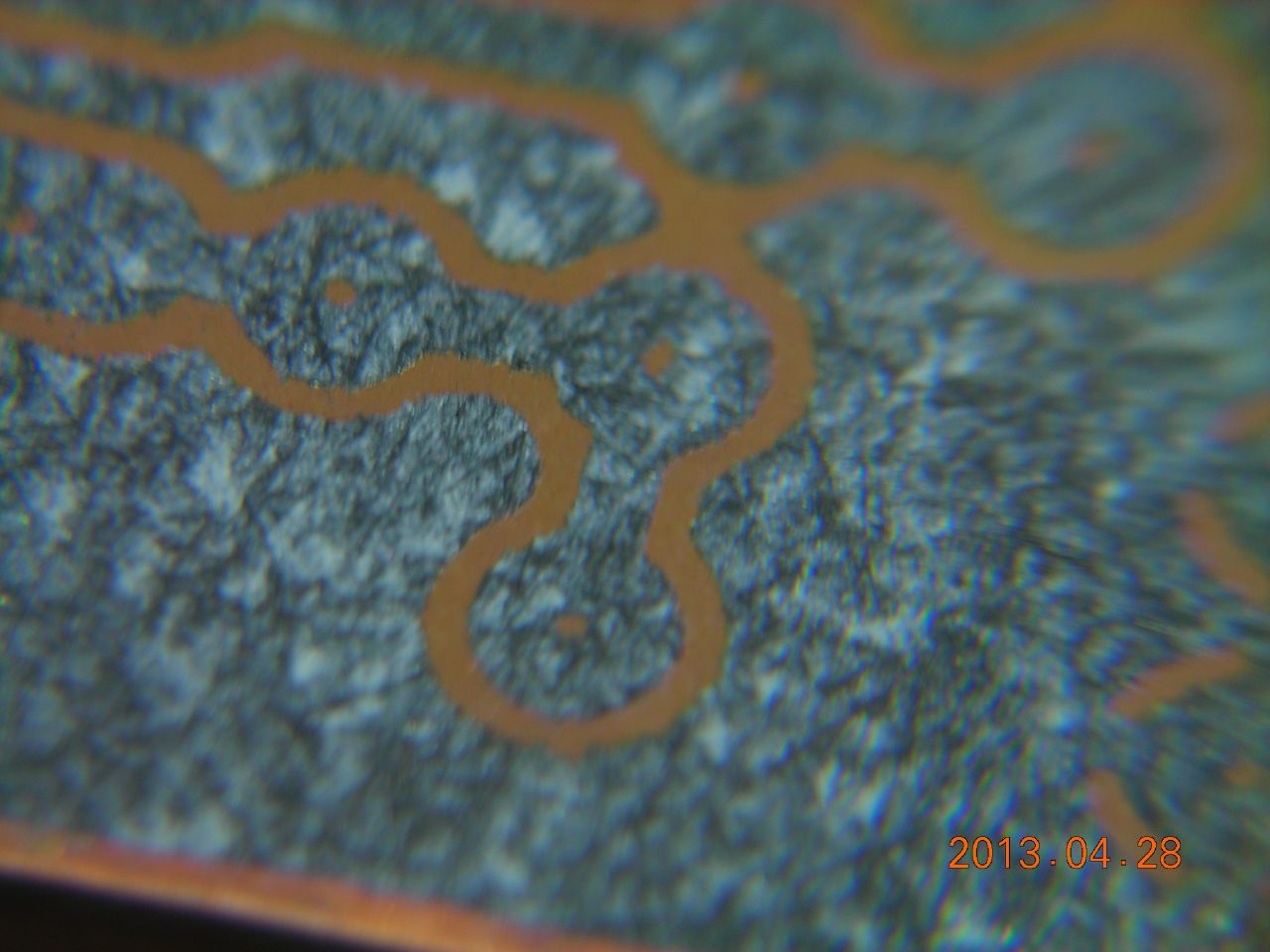
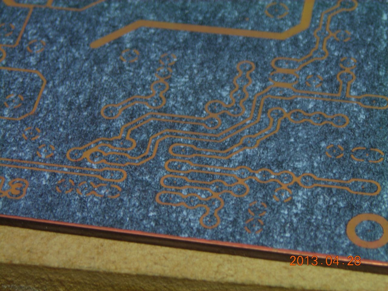 Closeup just after transfer |
 |
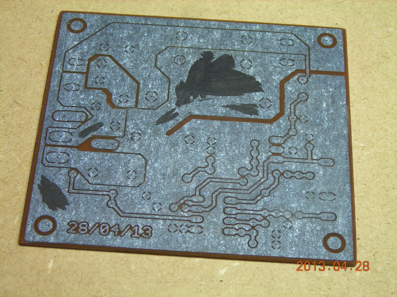
 Before etching - some areas touched up |
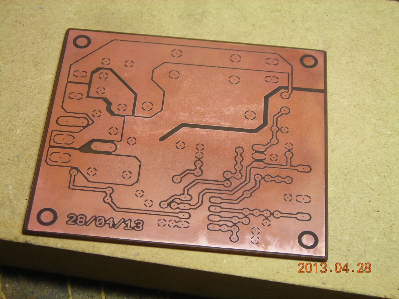
 After etching |
 Toner removed with acetone |
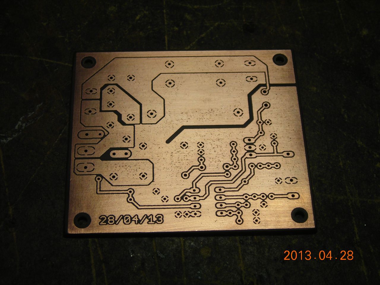 Board brightened up with abrasive block |
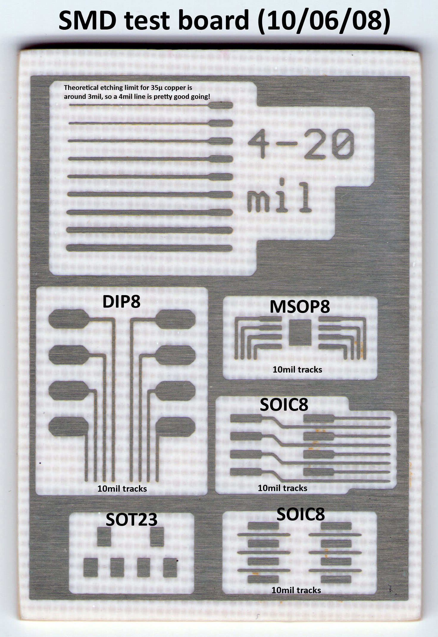
Firstly, here's a test board I did once with different sizes of tracks. The transparency for this was printed on a big office laser printer so is probably better quality than on my little one. Click here for the artwork (1200dpi JPEG).
 |
Now some general photos.
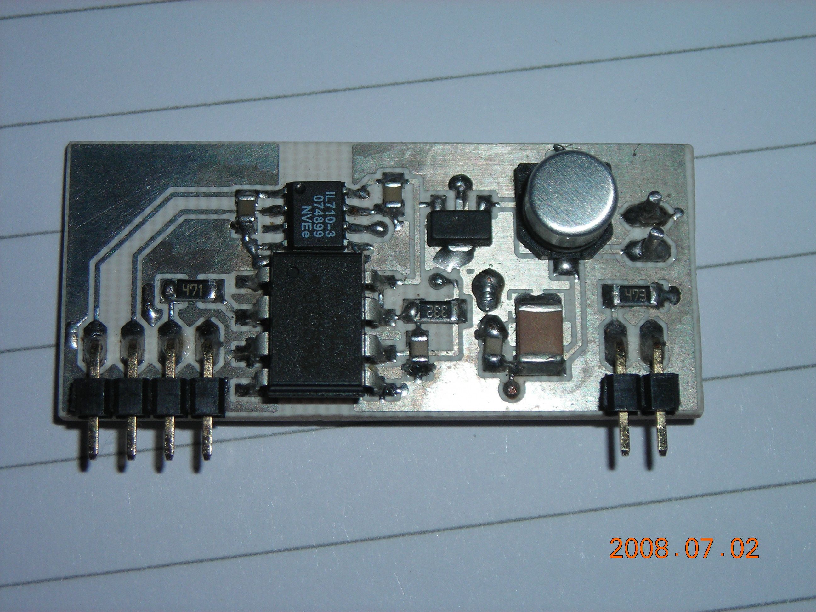 Small gate driver, tin-plated |
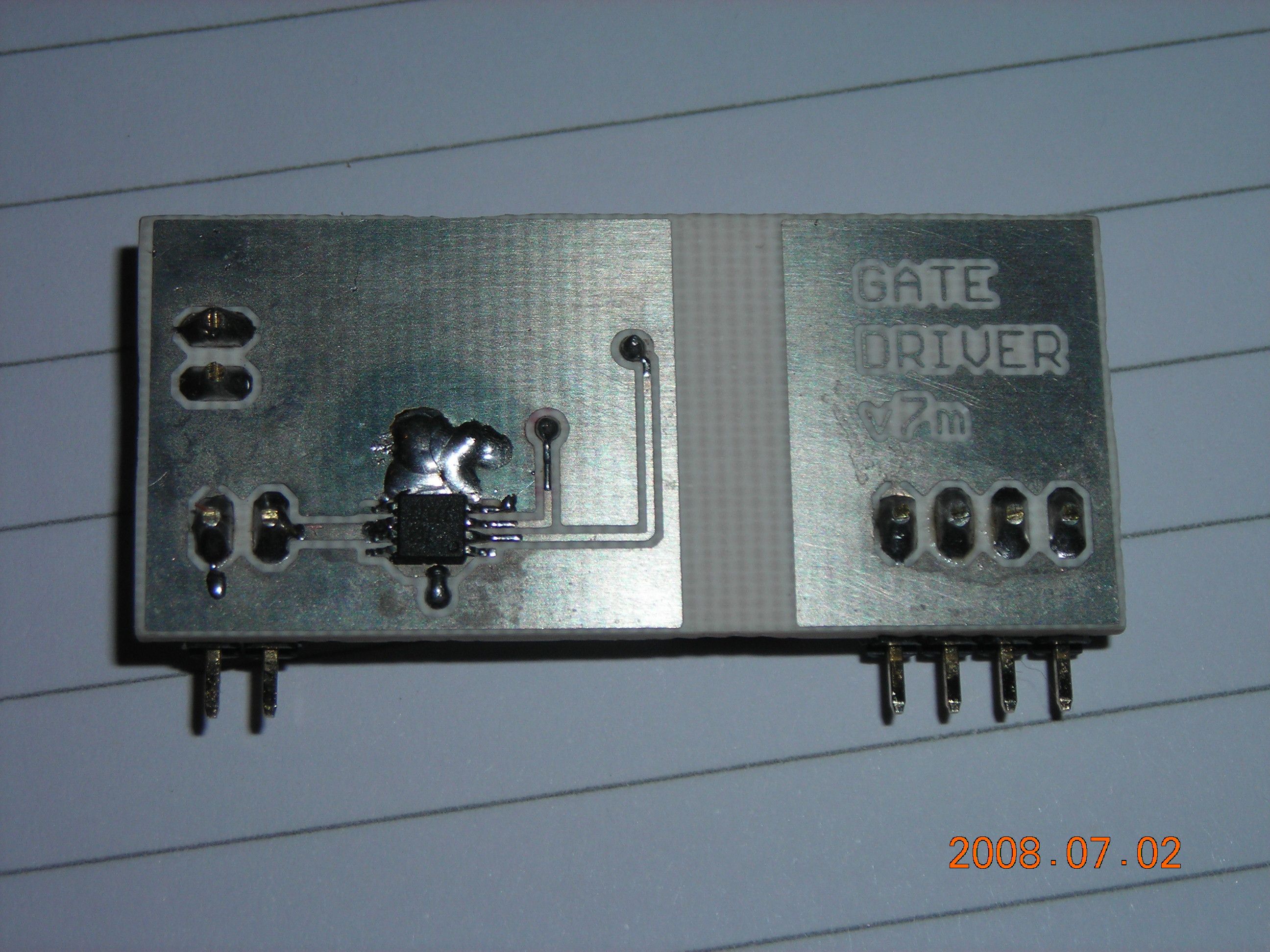 Reverse with MSOP8 driver chip (UCC37322) |
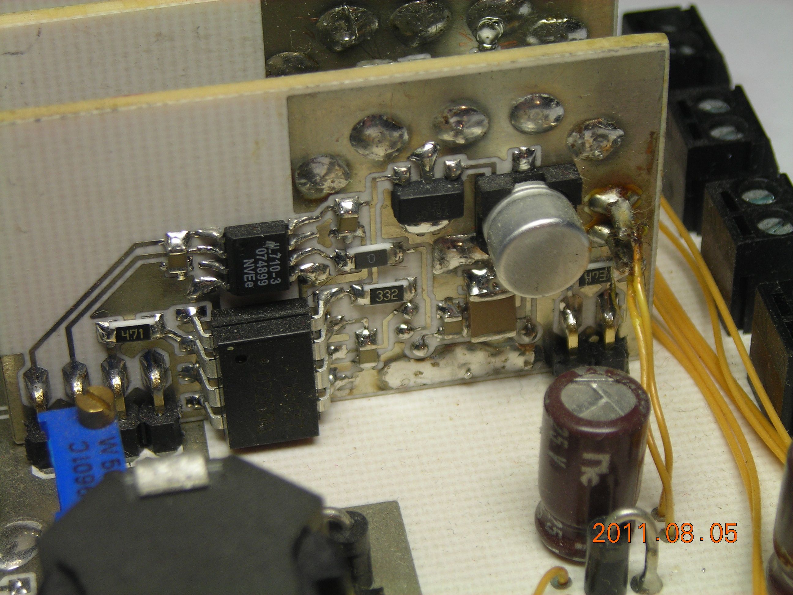 Mounted on carrier board (ignore hairy stuff) |
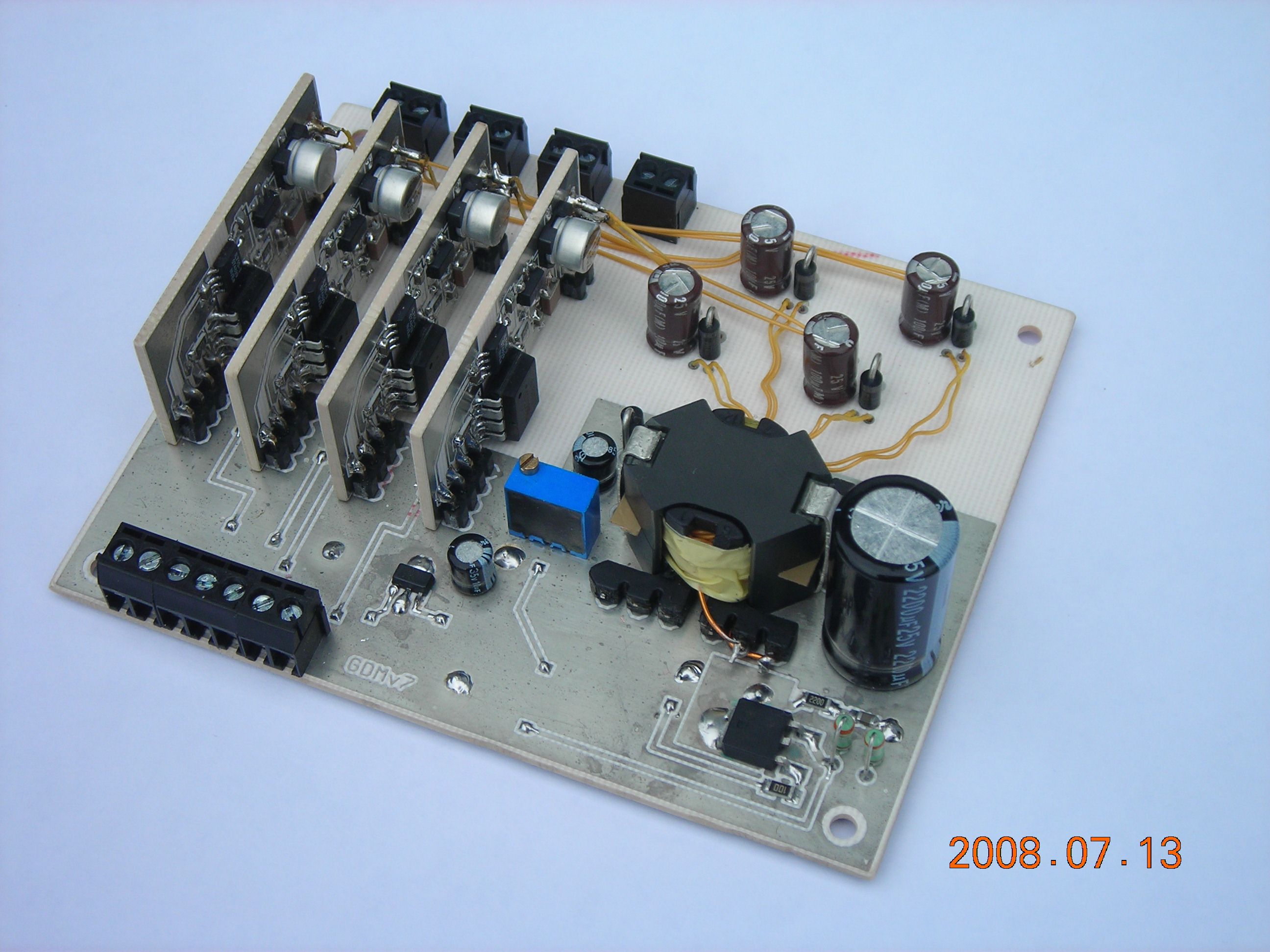 Carrier board - four channel |
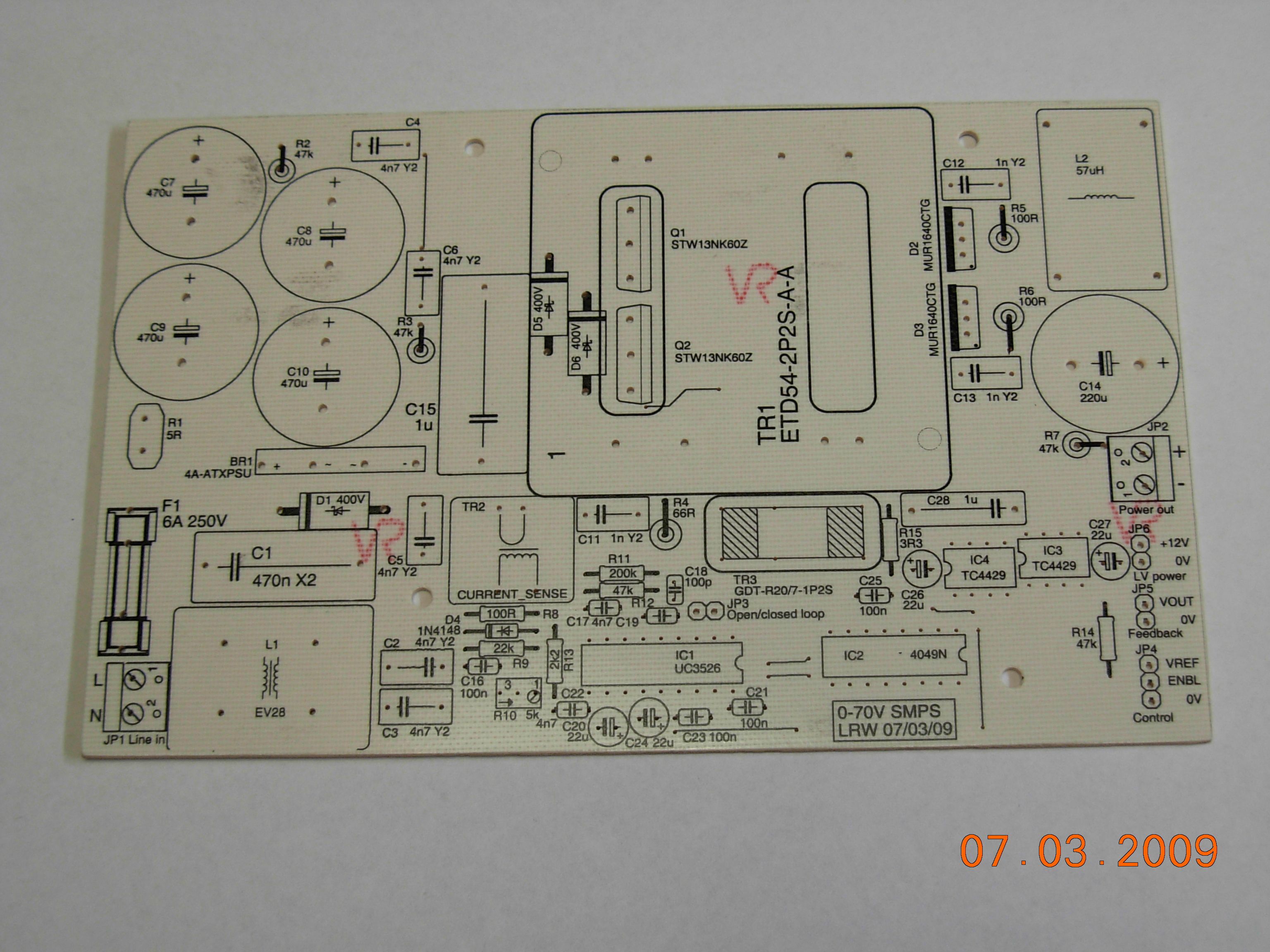
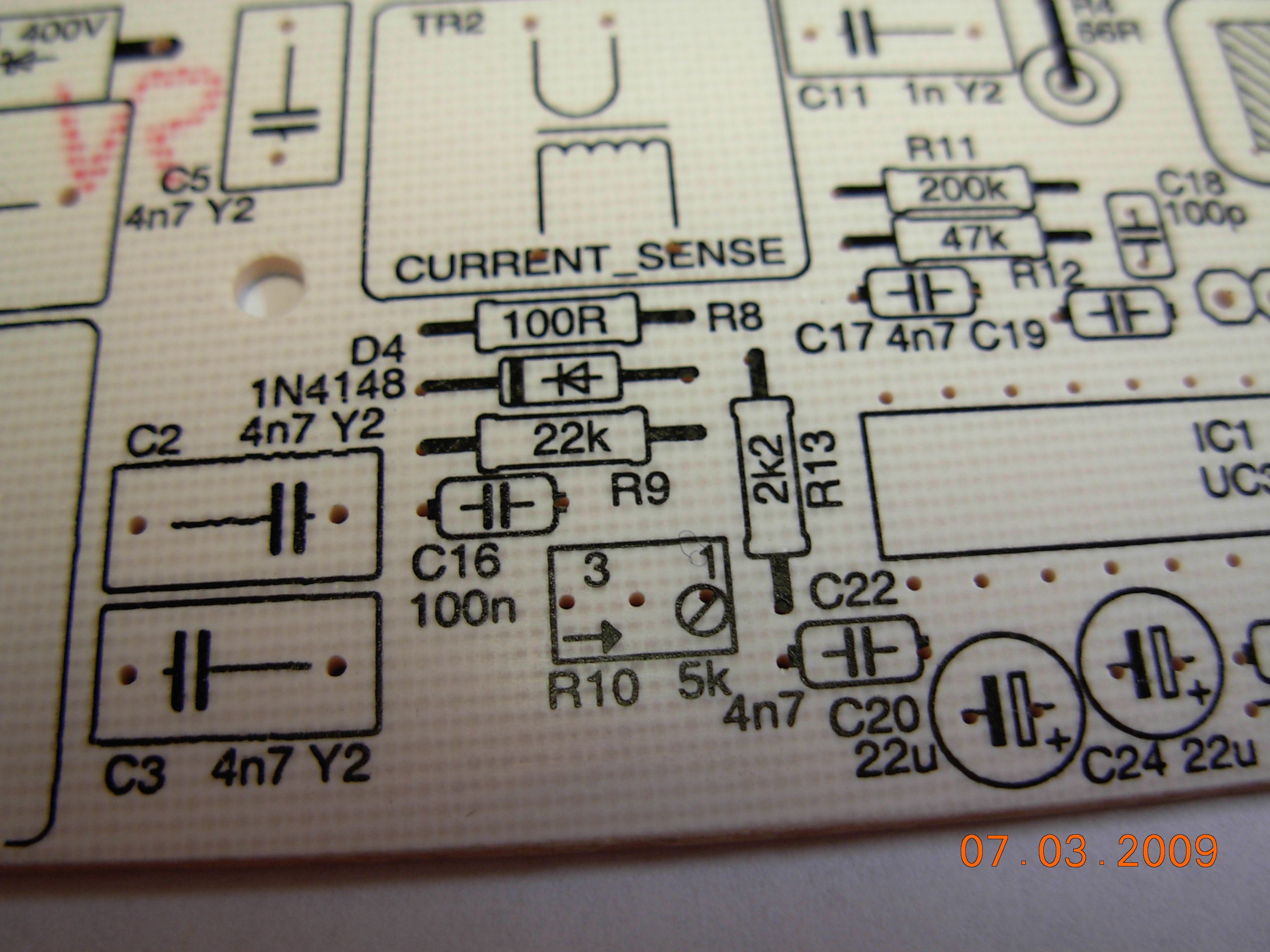
 Off-line 70V adjustable supply (didn't work!) |
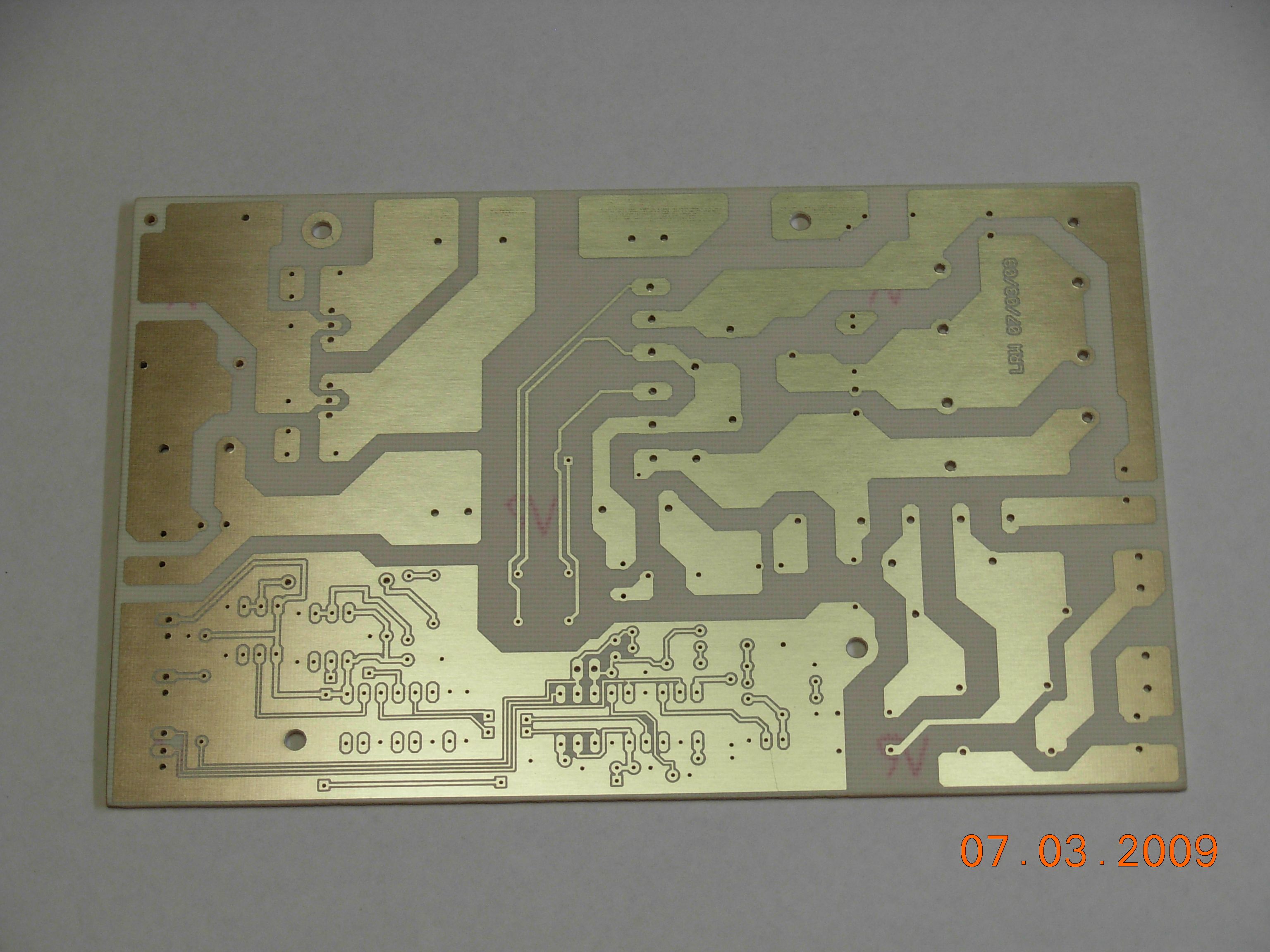
 Silkscreen layout - toner transfer |
 Closeup |
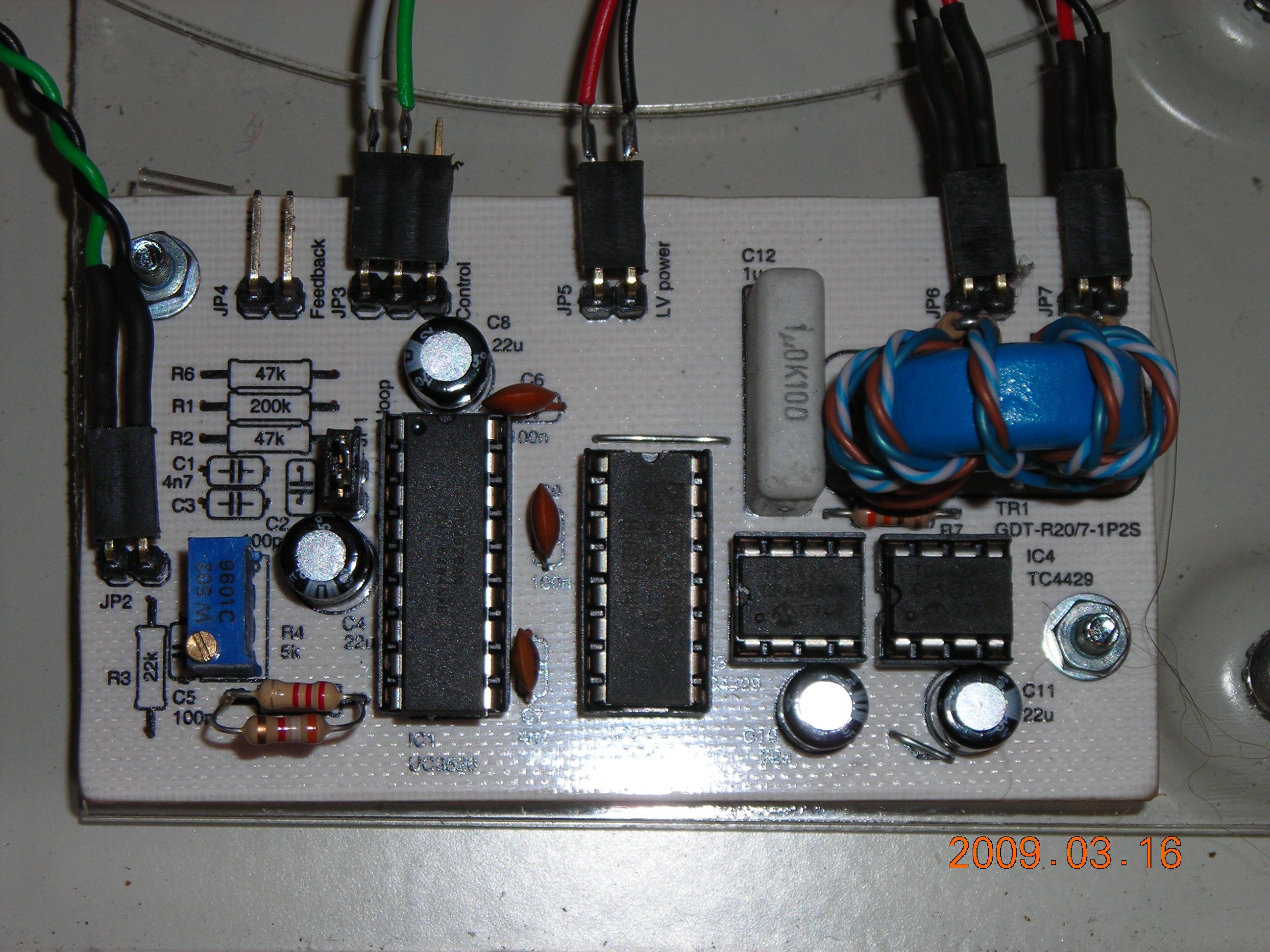 Separate controller board |
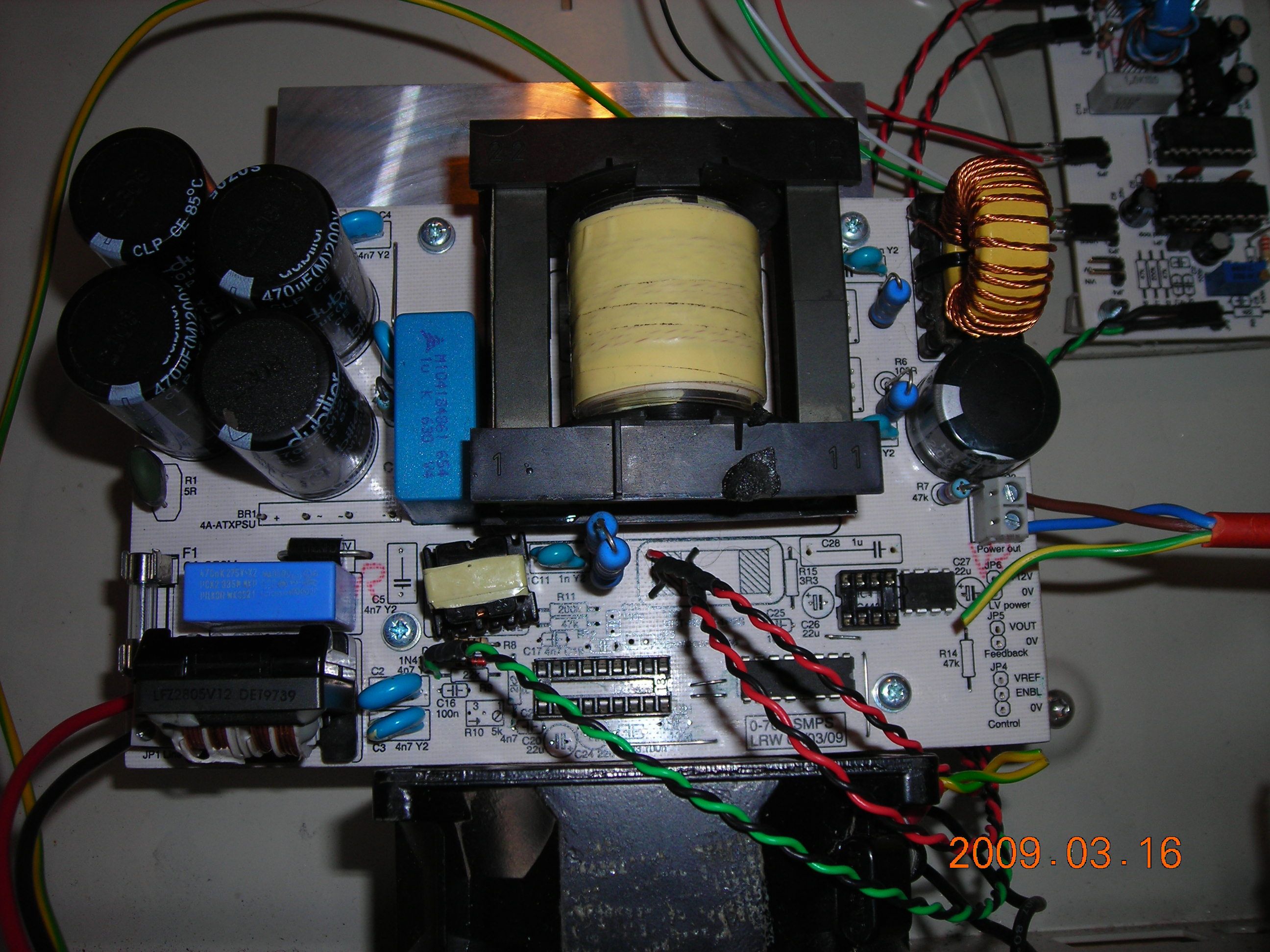 Main board populated |
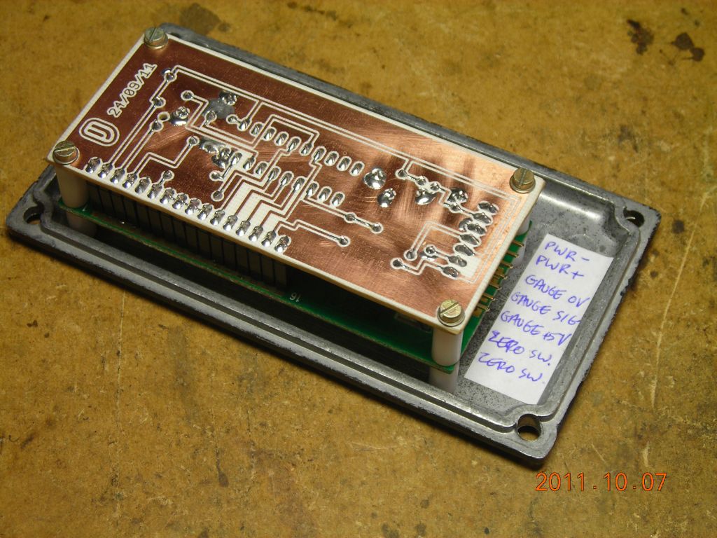 LCD driver "backpack" |
 40-400V adjustable HV supply |
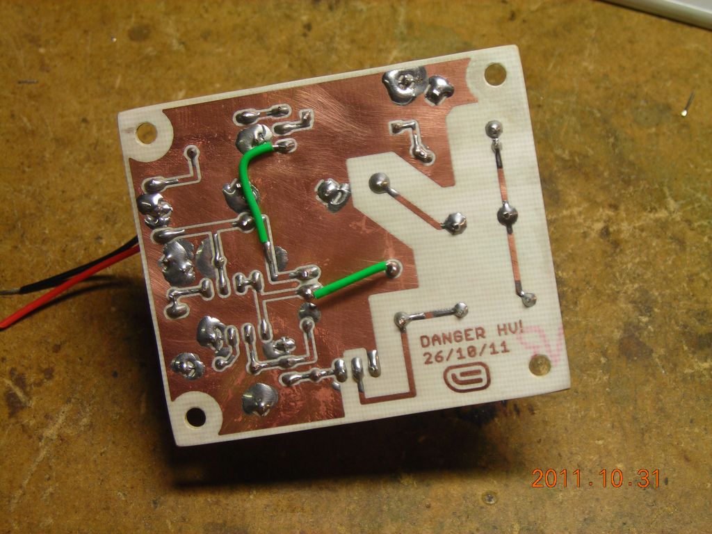
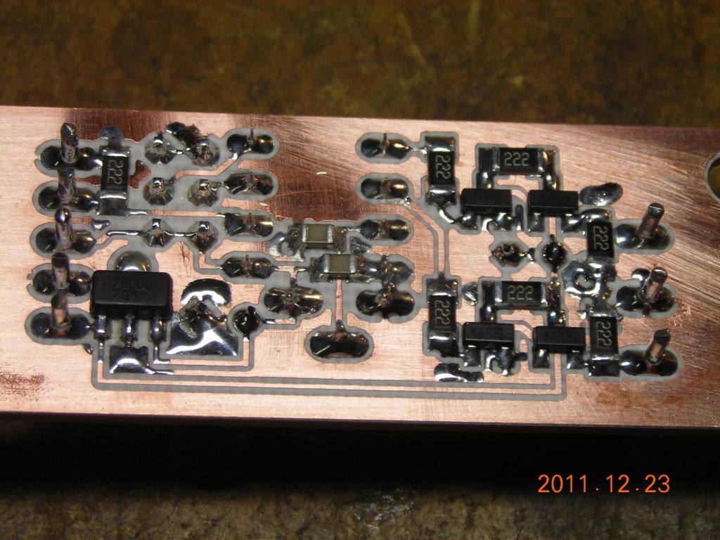 Dual-pulse trigger thingamajig |
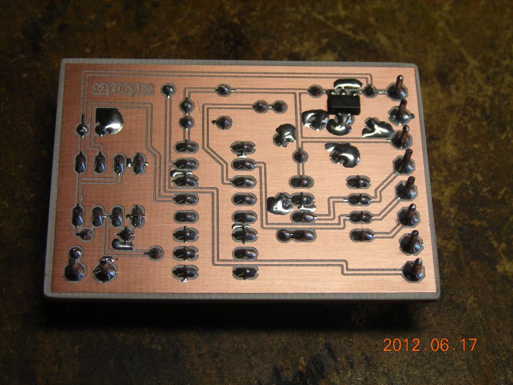
 Closeup of part of my IJ-6 temperature controller |
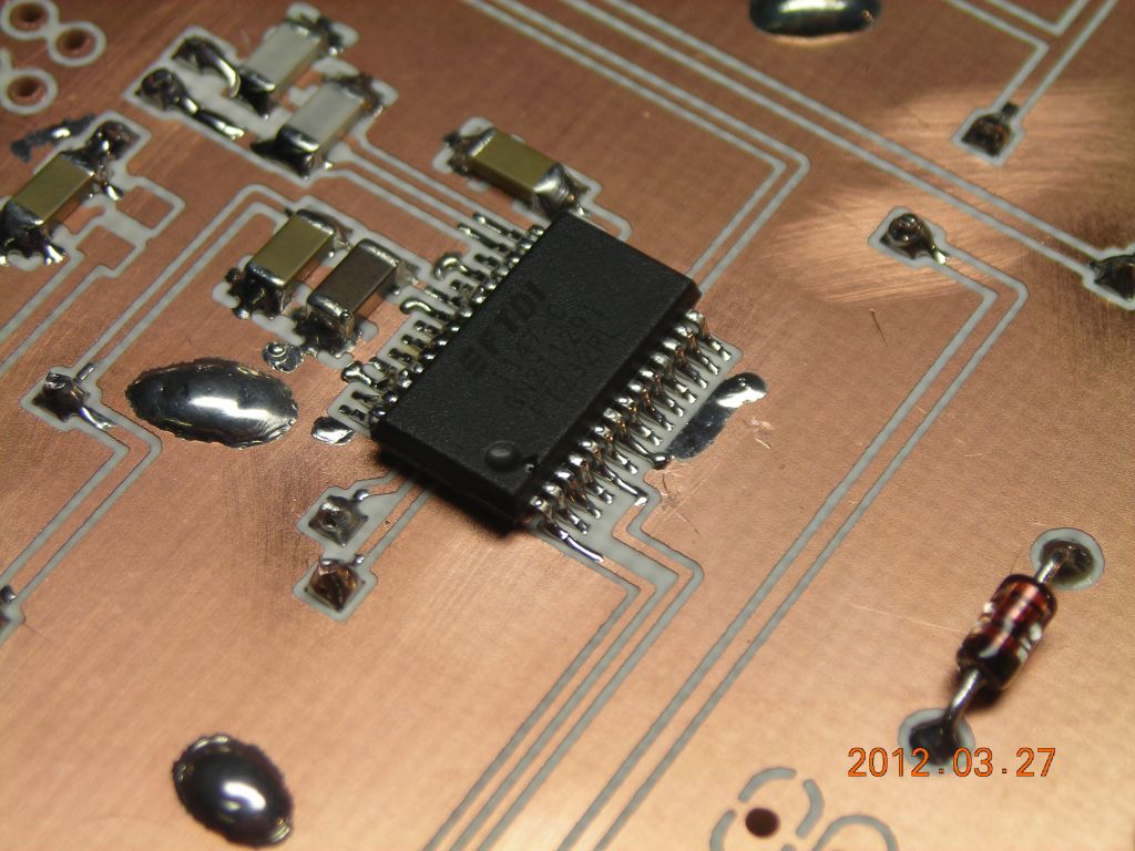 SSOP-28 chip soldered (FT232RL) |
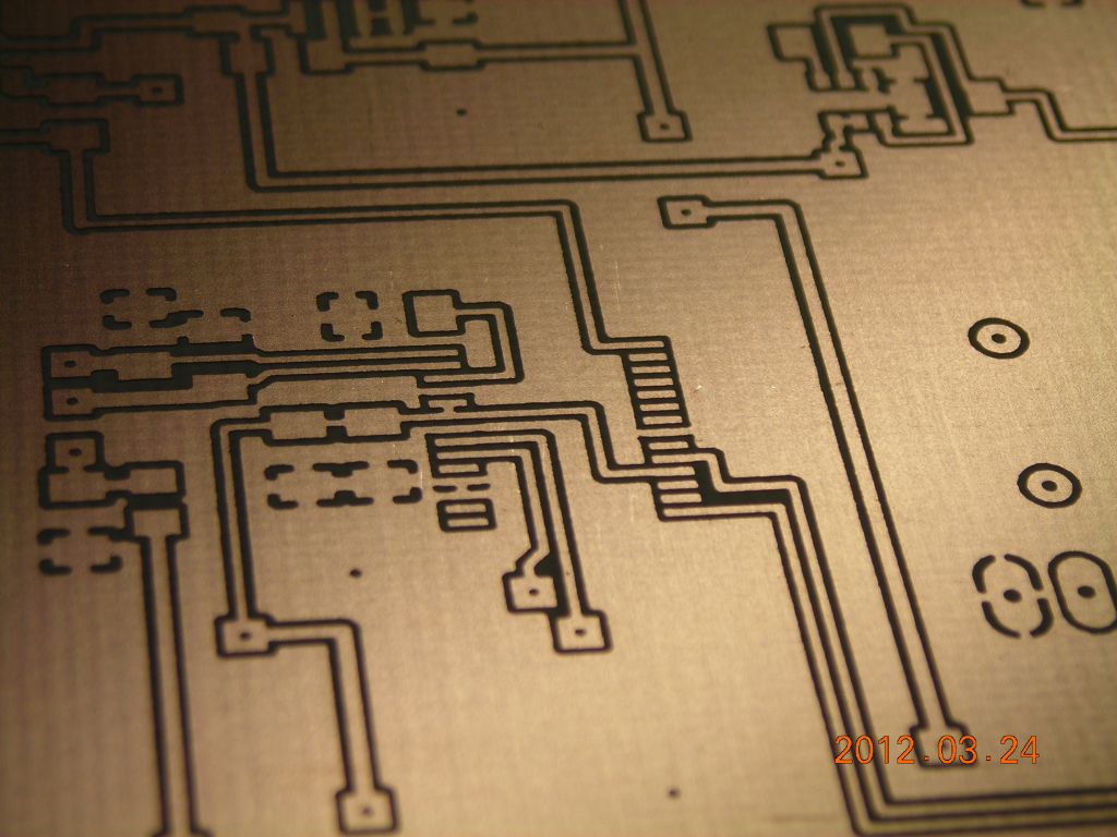
 Wide-range pulse generator |
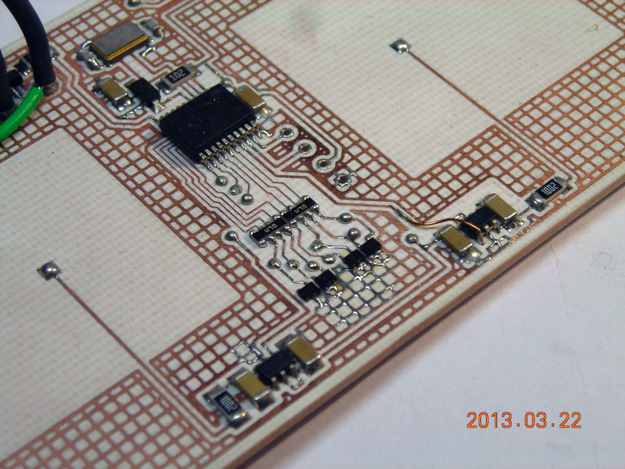 Something I'm working on at the moment. The tracks to the big IC were supposed to be 10mil but look thinner. Scale - the four small black things at the front are about 1.5mm. |
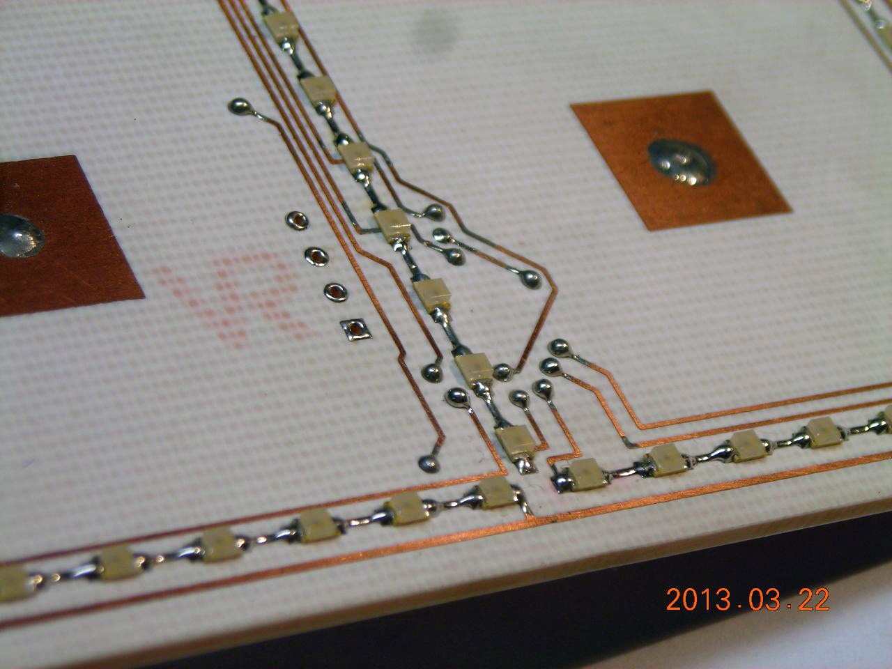 Other side of the board showing the LEDs. Note the vias - I managed to get a nice round blob. |
| ▲ Electronics |